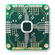
When routing high-speed signals that transition between layers, ensuring a low-inductance return path is critical for signal integrity and EMI control. Whenever a signal trace jumps through a via, its reference plane changes. If the accompanying return-path stitching via is placed too far away, the high-frequency return current is forced to ta...
follow.it gives you an easy way to subscribe to Altium PCB Designer's news feed! Click on Follow below and we deliver the updates you want via email, phone or you can read them here on the website on your own news page.
You can also unsubscribe anytime painlessly. You can even combine feeds from Altium PCB Designer with other site's feeds!
Title: Altium PCB Designer